Phase Shift Reticle Design
Exclusive: GaAs Mask
Benchmark Technologies has teamed up with Petersen Advanced Lithography (PAL) as the exclusive worldwide distributor of GaAs MASK™, with all rights to provide access to PAL’s patent for a novel phase shifting reticle enhancement technology. This technology is targeted at isolated trench applications, which are commonly used in Gallium Arsenide chip fabrication facilities. For many high performance RF applications, the gate length has effectively shrunk to feature sizes smaller than what is possible with conventional i-line wafer steppers and reticles. In many of these fabs, critical gate layer lithography is performed using electron beam lithography which suffers from lower throughput and higher costs.
The GaAs Mask™ approach extends i-line (365nm) stepper tool capability into the deep sub-wavelength regime, allowing the user to print features that may be 30% or even smaller than possible with conventional reticles. The approach can be used at other wavelengths such as 248nm and 193nm, but for most GaAs fabs, extension of the 365nm tools is the higher priority.
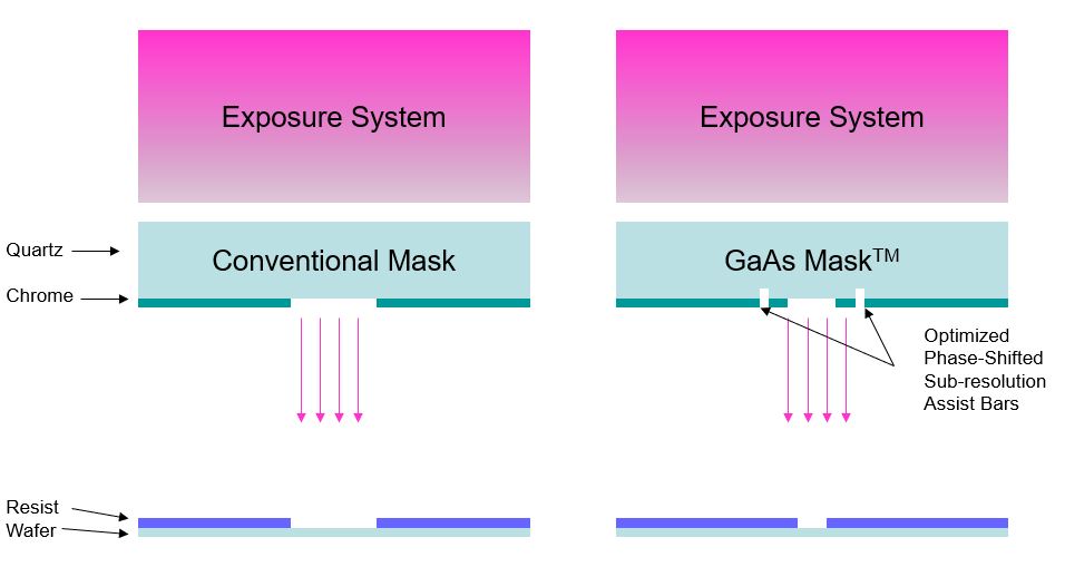
A GaAs MASK™ reticle differs from a conventional reticle due to the addition of phase shifted sub-resolution assist features (PS-SRAF) as shown in the schematic. The critical parameter is selection of the size and spacing of the of the PS-SRAF, the determination of which is the result of rigorous simulation of the entire lithography process using proprietary and patented techniques. The simulation considers the exposure tool, its available settings and the photoresist stack. We also insist some experimental data be collected off of printed wafers using a multi-variant test reticle prior to integration into production reticles. There are some wafer-steppers used in GaAs fabs today that are not compatible with the technique due to either fixed NA or fixed sigma settings. Please contact us to discuss the compatibility of your tools for GaAs MASK™ integration.
The advantage of GaAs MASK™ is the ability to resolve smaller features using the same lithography tools as the other less critical layers. By replacing the e-beam approach with GaAs MASK™, the user can negate the need to update or replace an aging e-beam writer or continue with costly maintenance. Furthermore, I-line wafer steppers are ubiquitous and have been integrated into the broader CMOS market for over 25 years, making parts and full systems readily available on the used and refurbished equipment market.
On the technical side, the GaAs MASK™ technology provides the user with greater exposure latitude and more useable depth of focus, allowing for a robust manufacturing process. The simulation shown here for a 220nm line shows ~21% increase in DOF and ~40% increase in exposure latitude when a GaAs MASK™ reticle is compared to a conventional binary intensity mask. Of course, this is an integrated lithography approach, so the results are dependent on the user’s litho tool, resist stack and available tool settings.
If you want to extend your i-line tools or discuss a project at lower wavelengths, please contact us to explore integrating GaAs Mask into your lithography flow.
Other PSFM Services
In addition to our exclusive GaAsMask design service, we also offer other phase shift mask types including: alternating aperture, phase edge with trim and embedded attenuated (MoSi). Please contact us for more information